
EUV Lithography
EUV lithography uses extreme ultraviolet light at 13.5 nanometers to print the circuits on the world's most advanced computer chips.
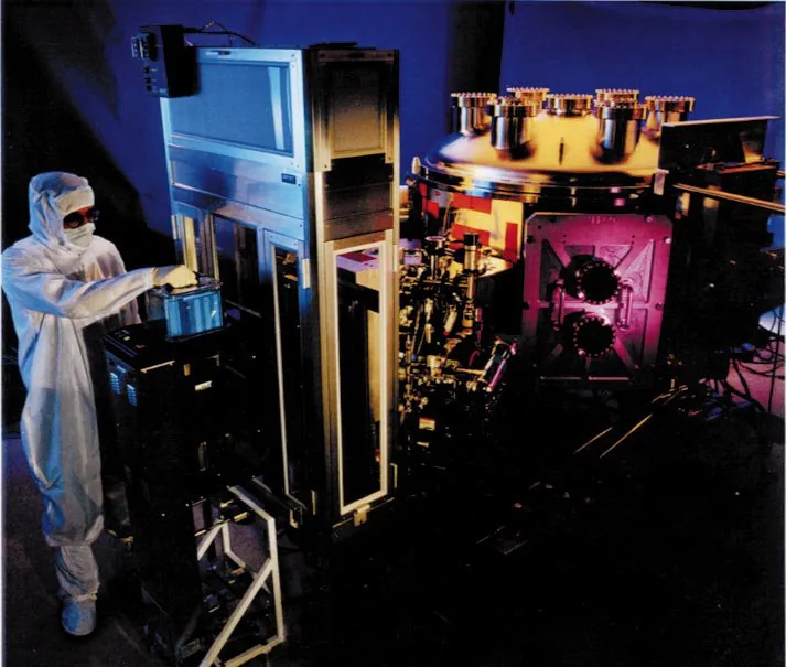
EUV lithography is a chipmaking technology that prints circuit patterns using extreme ultraviolet light at a wavelength of 13.5 nanometers. That is about fourteen times shorter than the 193-nanometer light the industry used before, and short enough to draw transistors just a few dozen nanometers wide. Each machine costs between $150 million and $400 million, weighs more than 150 tons, and contains roughly 100,000 parts. Only one company builds them: ASML, a Dutch firm headquartered in Veldhoven, a small town in the south of the Netherlands. Taiwan's TSMC, Samsung in South Korea, and Intel in the United States are among the few chipmakers running EUV machines in volume production. Without this tool, no factory on Earth can make the most advanced chips inside the latest phones, AI servers, and data centers.
How EUV lithography was developed
No single person invented EUV lithography. Hiroo Kinoshita, a physicist at Nippon Telegraph and Telephone in Japan, produced the first EUV images in 1986 and is widely recognized as the technology's pioneer. Around the same time, Obert Wood at Bell Labs in the United States was developing EUV light sources independently, and researchers at Lawrence Livermore National Laboratory began their own program soon after. The logic was straightforward: shorter light draws finer lines, and Moore's Law demanded finer lines every couple of years. The problem was that 13.5-nanometer light is so energetic that air absorbs it, and so does ordinary glass. A working machine would need a near-perfect vacuum, mirrors instead of lenses, and a light source that did not yet exist.
For most of the 1990s and 2000s, much of the chip industry believed EUV would never leave the laboratory. ASML bet that it would. The company joined a research consortium with American national laboratories including Lawrence Livermore and Sandia. It bought its American laser supplier, Cymer, for $2.5 billion in 2013 and took a billion-euro stake in the German optics firm Zeiss, which makes the machine's mirrors. In 2012, ASML sold a combined 23 percent of itself to Intel, TSMC, and Samsung for about 3.85 billion euros as part of a deal to help fund the work. No single company could afford EUV development alone, so ASML financed key parts of its supply chain.
The first machines shipped for testing in 2006 but were too slow and unreliable for a factory. TSMC began using EUV in high-volume chip production in 2019, at the 7-nanometer process node, more than thirty years after Kinoshita's first demonstration. Why ASML ended up as the only company that builds these machines comes down to a bet its Japanese rivals, Nikon and Canon, eventually abandoned.
How does an EUV machine work?
The machine generates its light by directing a powerful carbon dioxide laser at drops of liquid tin, each roughly 25 micrometers in diameter. The laser hits roughly 50,000 droplets every second. Each droplet is heated into a plasma that emits light at exactly 13.5 nanometers. Only a small fraction of the laser's energy converts into usable EUV light, which is one reason the machine draws over a megawatt of electricity.
Because EUV light cannot pass through glass, the machine uses a series of curved mirrors instead of lenses. The mirrors are coated with alternating layers of molybdenum and silicon and are the flattest surfaces ever manufactured. If one of these mirrors were enlarged to cover the area of Germany, its tallest bump would be about a tenth of a millimeter high. The light bounces off these mirrors and off a patterned plate called a reticle, which casts the chip's circuit design onto a silicon wafer coated with a light-sensitive material.
The entire process happens inside a near-perfect vacuum. A finished machine contains around 3,000 cables and two kilometers of tubing, and ASML ships each one in roughly forty freight containers. In 2026, a standard EUV machine costs about $200 million. The newest version, called High-NA, uses a wider-angle mirror system for even finer patterns and costs about $350 million to $400 million.
EUV lithography and the US-China chip war
Since 2019, the Dutch government, under pressure from the United States, has refused to let ASML sell any EUV machine to China. Not a single EUV scanner has ever reached a Chinese factory. The United States sees the restriction as a way to keep China a generation behind in advanced chipmaking. China sees it as proof that the technology has become a tool of foreign policy.
China has spent heavily on building its own EUV capability. The Chinese government organized more than 3,000 researchers across institutions including the Harbin Institute of Technology, the Changchun Institute of Optics, and the state-backed lithography firm Shanghai Micro Electronics Equipment, known as SMEE. In early 2025, a team in Shenzhen built a prototype EUV light source, but it produced only 100 to 150 watts of EUV power. ASML's current machines run at about 600 watts. SMEE itself has only reached mass production of tools working at 90 nanometers, many generations behind the cutting edge. Most independent analysts say China is unlikely to produce working EUV chips before 2030 at the earliest.
The restrictions keep expanding. In 2026, the United States pushed the Netherlands to block exports of almost all of ASML's older, non-EUV machines to China as well. A technology that took thirty years to move from laboratory to factory now determines which countries can make the most advanced computer chips.